


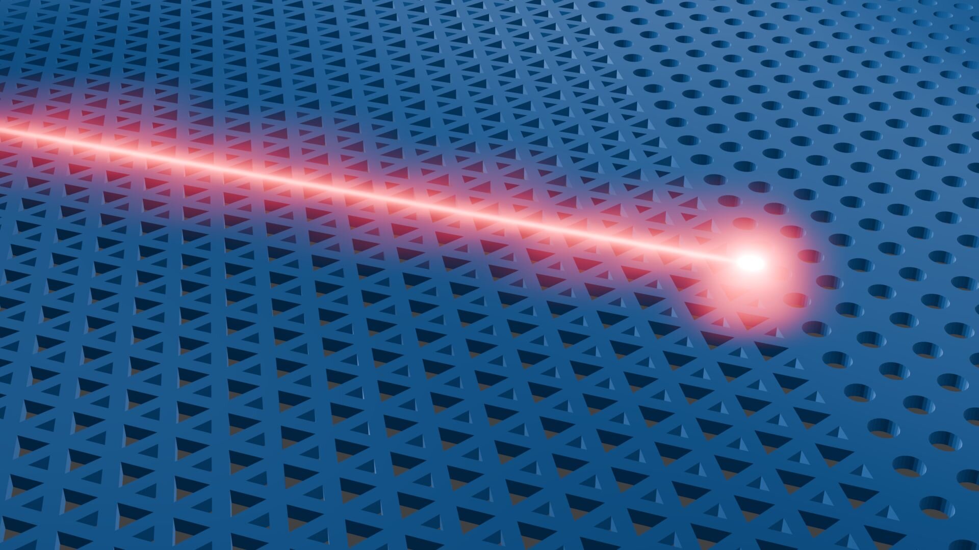
Artist’s impression of the light concentration at the ‘wall’ at the end of the waveguide. Credit: AMOLF
Harnessing the Power of Light at the Nanoscale
In a significant advancement for photonic technology, researchers from AMOLF, TU Delft, and Cornell University have unveiled a new mechanism to concentrate light on a chip using photonic crystals. This method allows for the amplification of light in volumes as small as its wavelength, a feat that holds promise for various applications in quantum communication, optical sensing, and on-chip lasers.
The Challenge of Light Concentration
Concentrating light into minuscule volumes is essential for enhancing the performance of photonic devices. Traditional methods involve optical cavities or waveguides, each with limitations concerning wavelength specificity and device size. The new approach leverages the unique properties of photonic crystals to overcome these challenges.
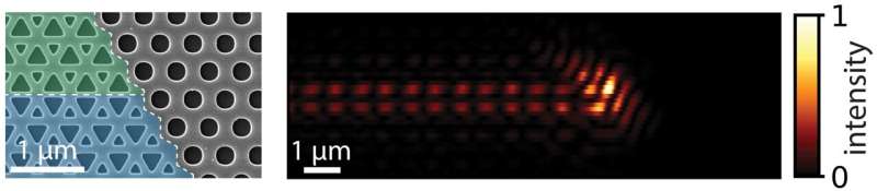
Left: An electron microscopy image of the silicon photonic crystal. The topological waveguide is formed at the boundary between the green and blue regions, and is terminated by the crystal with round holes on the right side. Right: A measurement of the optical intensity in the photonic crystal. Light enters through the topological waveguide from the left and accumulates at the end of the waveguide due to suppressed back reflection. Credit: AMOLF
Innovative Use of Photonic Crystals
Photonic crystals are structures with periodic variations in refractive index, which affect the motion of photons. By creating a waveguide at the boundary between two photonic crystals with mirrored patterns, researchers established a path where light can travel with minimal scattering. Terminating this waveguide with a “wall” causes light to accumulate at the endpoint due to suppressed back reflection, resulting in localized amplification of the light field.
Experimental Validation
The team fabricated the topological waveguides on silicon chips and employed a specialized microscope to observe the light concentration. The experiments confirmed that light intensity increased significantly at the waveguide’s termination point, validating the theoretical predictions. This amplification occurs over a broad spectrum of wavelengths, making the technique versatile for various photonic applications.
Implications for Future Technologies
This discovery opens new avenues for developing compact and efficient photonic devices. The ability to concentrate light in such small volumes could lead to advancements in quantum computing, high-resolution sensors, and more efficient on-chip lasers. The method’s broadband nature ensures its applicability across multiple technologies, potentially revolutionizing the field of integrated photonics.
Curious to Learn More?
How might this breakthrough in light concentration influence the next generation of photonic devices? Stay tuned to DailySciTech.com for the latest updates on this and other exciting developments in science and technology.